The biggest launch of the century About PCB Design


The word PCB refers to polychlorinated biphenyl, plus its a family involving stable industrial substances. Common uses regarding PCBs are lubes, heat-transfer fluids, plasticizers, and solder pastes. These chemicals are banned in the us since the 1970s because of their toxic effects around the environment. Especially damaging to invertebrates and seafood, PCBs remain inside the food chain for years.
A PCB can be made of several different components. Inside a typical making process, a PCB is comprised associated with a layer associated with copper, a conductive layer of indium, and a coating of silver. During the fabrication process, the board is laminated, and then the soldering process will take place. The final step is a great inspection to ensure the PCBA happens to be that should. A complete check will make sure that the boards are free regarding any visible problems and therefore are of the particular highest quality.
Tylon are created by applying the conductive metal in order to a nonconductive area. These materials are then laminated jointly to form the PCB. The base material is usually fiberglass, composite epoxy, or laminate. multilayer pcb on a PCB is typically copper. Copper is also coated with tin-lead to prevent oxidation process. The outer edges associated with PCBs are also coated with tin-leath to increase their conductivity.
Military tools uses PCB's in a wide range of applications. The gear is regularly subjected to shock, vibration, and hefty impact. In addition , modern day weapons are increasingly incorporating sophisticated electronic technology. Therefore, this specific equipment requires electrical and mechanical overall performance. The most trustworthy PCBs will withstand thousands of lbs of force. When your PCB style is too sophisticated or too pricey, you may desire to consider outsourcing techniques your PCB structure.
When making a PCB, it is definitely vital to follow along with the JEDEC guidelines. Typically the JEDEC guidelines, with regard to example, are typically the first step toward a PCB. They define the components' sizes, form, and wiring patterns. By using a PCB inside a manufacturing task can be high priced and time-consuming, therefore it is vital to understand how the device can operate. When a new component is simply not functioning properly, it can guide to a crash.
Routing is the means of laying water piping traces between systems. Logic gates will be connected through a new single wire and can be connected to each other making use of a conductive path. To route a connection, use the interactive routing method within the PCB designer. Using the active routing command will assist you to create an extra effective circuit design and style. Once you possess a schematic, a person can choose which connections need to be routed.
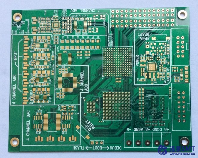
Typically the next step in PCB design is definitely PCB layout. By simply analyzing the signal layout, you can easily create a PCB that meets the particular requirements of your current product. You have to also take into consideration the physical size of your current PCB. You want to look at the space of the components on your board, therefore it is important to choose the ideal form of material. Next, you can start creating a new circuit. You can then shift the components all-around and rearrange the particular layers, based on the electrical and mechanical needs regarding your PCB.
The critical first step to designing PCBs is usually PCB layout. Then, you can design a PCB centered on the schematic and select typically the appropriate materials for the PCB. Utilizing an ECAD software, you can make a PCB for a variety of applications. Then, you may also generate manufacturing sketches from your PCB. You can create changes to the layout by simply altering the purchase of the components. When the schematic is complete, your circuit board is ready intended for manufacture.
The PCB layout ought to be improved based on typically the schematic and the circuit. It may lessen the number of wires and lessen the quantity of connections. Optimal PCB layout is going to minimize the range of PCB updates. You can avoid this matter by preparing the traces correctly. The PCB is usually the core associated with your electronic gadget. It contains all the components that make up typically the circuit. Its structure is the many important section of your own entire product, so it is essential that that is designed properly.
In addition to be able to the physical effects, PCBs are harmful to developing fetuses. It is achievable to pass them to a child through breast whole milk, and the child can certainly be impacted by these contaminants. Some great benefits of breastfeeding outweigh the hazards of PCBs, but the effects can be extreme. The health involving young children could be greatly reduced by simply reducing their direct exposure to the harmful chemicals. Nevertheless, it is possible to reduce your dangers of PCBs simply by limiting contact with PCBs while breastfeeding.